

Gameboy Reverse Engineering & Hacking - Part2
Part2:
In Part1 we touched on the basics of dumping an unknown ROM, looked through the code to see how it controls its peripherals, used the Joey to replicate and manipulate the newly discovered registers and had a look how they work at the most basic level.
This is what we found:
- $0000 – Not certain if it is more than just SRAM enable/disable
- $1100 – Used to select 512kbyte banks, 32k SRAM banks & Cart bypass mode.
- $3100 – Important but unknown
- $4100 – Important but unknown
This is a good start. Before we can get really deep we need a thorough understanding of how a cart like this does what it does.
The Gameboy has an 8-bit CPU with a 16bit address bus. This allows the CPU to address up to 65,536 unique memory locations. The upper half of this is dedicated to internal CPU/Gameboy registers like LCD and Sound control registers, Internal RAM both video and general purpose and various important system registers. This leaves us with 32k of address space to access our ROM and any peripherals the cart may contain.
Banks:
Games like Tetris were coded to fit within this 32k and the entire ROM could be accessed by the Gameboy as it was needed. For many developers 32k was simply not enough. A cheap and effective way of expanding the 32k limit was needed and Nintendo (and various pirates) used similar techniques found in the NES cartridges - Mappers.
Nintendo split the ROM space into 2 banks, 0 & 1. Bank0 remains permanatly 'mapped' to the first 16kbytes of the ROM data. Bank1 can be re-mapped to different 16kbyte regions throughout the entire ROM. 2 banks were chosen due to engineering simplicity. The most significant bit (MSB) of the 64k address (A15) will now indicate if cart I/O or internal I/O is requested. A14 will indicate if Bank0 or Bank1 is to be selected.

Using this same principal, we can detect when a particular address is being accessed. Our cart does this to detect writes to addresses $1100, $3100 and $4100.
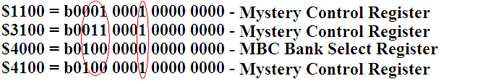
We can see any access with A8 High indicates access to a Mystery register. If A8 is high we can then look at the value of A14-A12 to see which particular register is accessed. Using a handfull of logic gates (or a CPLD) we can easily build a ROM select mapper to swap out various 512kbyte ROM regions just as our cart does.
When approaching a design like this it often helps to think how the engineer would have thought. We need the most cost effective solution to the problem. We need to consider things like:
- How many ROM's do we want to store on the cart (4)
- What is the largest size of the ROM (2mbytes)
- Can variable ROM sizes be stored (Yes but must align to 512kbyte boundaries)
Using this information we could draft up a schematic that would not only be almost identical to what is acutally used in our cart, but also give insight into what kind of registers we would need to achieve our goal. There aren't *that* many ways to skin a cat.
Complex Programmable Logic Device - CPLD
A CPLD can be considered a large matrix of logic blocks. Each block is made up of a combination of gates and latches. The connection of these blocks is user definable enabling almost any gate combination you can dream up. There are a few ways for a coder to stitch these gates together, a text based language (VHDL, Verilog) or from a visual perspective (schematic). VHDL and Verilog are languages which describe the function of the device. If you have never worked with a CPLD/FPGA it can be confusing to get your head around the fact that all the 'code' runs simutaneously and not sequentially like in a CPU.
CPLD's come in various sizes and generally more logic blocks = more $$$. FPGA's are very similar though they work a little different. They are typically not 'instant on' devices and need to download their code from an external memory before they know what to do. FPGA's can contain up to 4 million logic blocks, run at many hundreds of MHz if not GHz and can be extremely expensive! Entire Gameboys have been tucked away into an FPGA, along with a NES, Sega and various retro consoles. The fastest code breaking / bitcoin mining computers are also made from these. Very cool devices.
Reversing the Engineering
From what we learnt in part1, we know the upper nibble at address $1100 controls SRAM 32k selection and Cart Pass-through mode and we know the lower nibble controls which 512K ROM Bank is selected. This should only require a handful of gates to recreate. This is what I came up with:

This is how it works:
- Any write to the cart I/O is accompanied by the /WR line being driven low
- The address from A15-A8 must be 00010001 to set inst2 high
- When inst2 is high and /WR is asserted, inst8 becomes active
- This latches the data on the bus into the latches
- This latched data directly controls the ROM + SRAM upper address bits.
- This is the entire $1100 register in our cart
The same would apply to the other Mystery registers in the cart, though they have a different purpose. The actual mbc5 mapper is a lot more complicated than this and we'll skip on it's operation. It is very well documented already.
1 register down, 2 more to go!
Out of interest, the CPLD used in the cart is an Altera EPM3064ALC44-10 which contains 64 'macrocells' and 34 I/O pins.
The flash ROM is a Sharp LH28F016SUT - a 2mbyte x 8bit or 1mbyte x 16bit Flash ROM.
The SRAM is a generic Sharp 128k x 8 low power static RAM.
See that 6 pin header at the top of the cart? That is for programming the CPLD. I have used Altera CPLD's in other projects (Homemade Gameshark for GB) so I have all the tools and software to reprogram this CPLD. Once we have all the registers documented, we can write our own mapper and upload it to the CPLD to see how close we get!
Also worth mentioning is that the BootROM has a finite size (reported 512k but measured at 10kbytes) , which means there is no longer 4 x 512k of ROM space for cart backups. It is a little bit less. Is this the reason behind register $3100? Find out in part3!
Thanks for visiting and don't forget to subscribe to my FB page for alerts on the next part of the series! If you would like more information on the tools/programs I use, or a more in depth explanation of how I do something, comment in FB. I'll get back to you ASAP.